Selective ablation, as an advanced laser processing technology, has demonstrated its unique application value and technical advantages in various fields. This technology uses lasers to precisely remove specific areas of a material's surface, achieving fine processing of the target region. In the selective ablation process, the interaction between the laser and the material is crucial. The laser's energy is absorbed by the material in the target area, causing rapid heating and subsequent evaporation or decomposition of that region. The ability to precisely control the laser's position, energy, and duration allows for accurate processing while minimizing damage to the surrounding material.
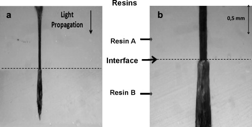
Figure 2. Microscopic photo of the ablation curve of the sample at the Resin A/Resin B interface
In the semiconductor industry, the application of selective ablation technology is particularly important. It is used in micro-etching of chips, especially for the manufacturing of fine circuit patterns. This technology is crucial for improving chip performance and density, as it allows for more precise definition of the size and shape of circuit elements, enabling higher integration and better electrical performance.
In the medical field, selective ablation technology also plays a key role. In laser retinal surgery and laser dental treatments, it is used to precisely remove damaged or diseased tissue. Compared to traditional surgical methods, selective ablation can more accurately target and treat the affected areas, reducing damage to healthy tissue and improving the precision and safety of the procedure.
In the field of materials science, selective ablation has shown its unique advantages in sample preparation and characterization. It is used to precisely cut and shape material samples for deeper chemical composition and physical structure analysis. This technology is crucial for understanding the fundamental properties of materials and for the development of new materials.
In MEMS (Micro-Electro-Mechanical Systems) manufacturing, the application of selective ablation is also essential. This technology is used to create miniature mechanical and electronic components, and its high precision machining capability is critical for manufacturing miniaturized devices and enhancing their performance. By precisely controlling the laser beam, complex miniature structures and components can be fabricated, which directly impacts the performance and reliability of MEMS devices.
In the field of cultural heritage preservation and artwork restoration, selective ablation also demonstrates its unique value. It can be used to clean and restore the surfaces of ancient artifacts, removing contaminants while preserving the original material. This method provides a non-invasive, high-precision cleaning and restoration technique for artifact preservation, helping to maintain the original condition and value of the objects.
In all these applications, femtosecond lasers play a vital role in selective ablation technology. The extremely short pulse duration of femtosecond lasers allows for highly precise material processing, minimizing the heat-affected zone and preventing damage to surrounding materials. This extreme precision and control make femtosecond lasers the ideal choice for performing high-precision and fine-scale machining.
The high peak power and precise pulse control characteristics of femtosecond lasers allow them to excel in processing various materials, whether hard materials (such as metals and ceramics) or sensitive materials (such as biological tissue and polymers). These features provide an efficient, precise solution for applications that require highly accurate and localized processing.
Overall, selective ablation technology, particularly when combined with femtosecond laser technology, has brought revolutionary advancements across various fields. From semiconductor manufacturing to medical surgery and cultural heritage preservation, this technology has demonstrated its powerful capabilities in precision machining and precise control, opening up new possibilities for future technological development and innovation.
References:
(1)Shuang-shuang Li et al. "Femtosecond laser selective ablation of Cu/Ag double-layer metal films for fabricating high-performance mesh-type transparent conductive electrodes and heaters." Optics Communications, 483 (2021): 126661. https://doi.org/10.1016/j.optcom.2020.126661.
(2)G. Nicolodelli et al. "Femtosecond laser ablation profile near an interface: analysis based on the correlation with superficial properties of individual materials." Applied Surface Science, 257 (2011): 2419-2422. https://doi.org/10.1016/J.APSUSC.2010.10.116.

 AI Assistant